Samsung, SK Announce $174 Billion Chungcheong Investment as Lee Recalls Founder’s 1983 Chip Bet
Summary
- Samsung said it will invest $101.5 billion in the Chungcheong region in cutting-edge displays, HBM fabs, next-generation batteries and package substrates for AI servers, while creating 250,000 jobs.
- SK hynix said it will invest $72.5 billion in Cheongju to expand M17, a NAND production fab, and P&T7, an advanced packaging facility, to respond to a surge in NAND demand.
- SK Group said it will build a 1GW AI data center in the Chungcheong region and combine that with a nationwide 15GW AI data center plan to strengthen synergies in the semiconductor and AI industry ecosystem.
Forecast Trend Report by Period


Lee Thanks Samsung and SK for Their Bold Decision
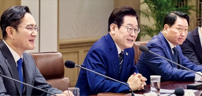
Samsung and SK Group on July 2 unveiled new investment plans for South Korea’s Chungcheong region, underscoring the area’s rise as a hub for advanced materials, components and AI semiconductors.
Samsung said it will invest 140 trillion won ($101.5 billion) in cutting-edge displays, high-bandwidth memory, or HBM, fabs, next-generation batteries and package substrates for AI servers. SK hynix said it will spend 100 trillion won ($72.5 billion) in Cheongju to expand a NAND production fab and advanced packaging facilities. As AI adoption lifts demand for high-performance memory, displays and package substrates, Chungcheong has emerged as a production base for advanced components and AI chips.
President Lee Jae-myung thanked the companies for the investment plans. Speaking on behalf of the public, he called the move a bold decision and said remarks by Samsung Electronics Chairman Jay Y. Lee reminded him of the historic moment when the late Samsung founder Lee Byung-chul declared the group’s entry into semiconductors in Tokyo in 1983.
Samsung announced the Chungcheong plan at a public briefing on the region’s advanced-industry development vision held at Samsung Display’s Asan campus. The company said the initiative is aimed at turning Chungcheong into a base for advanced materials and components and creating 250,000 quality jobs.
The investment has four main pillars. Samsung Display will complete a cutting-edge display cluster in Asan. Samsung Electronics will build what it described as a next-generation HBM hub through fab investment. Samsung SDI will set up a mother line to spread next-generation battery technology globally. Samsung Electro-Mechanics will seek to build a global manufacturing hub for high-performance package substrates.
In Asan, Samsung Display will expand its organic light-emitting diode, or OLED, production base. The company plans to add high-value OLED lines for smartphones and IT devices, as well as for XR, automotive, humanoid and wearable applications. The move is intended to meet demand for next-generation displays as AI, XR, robotics and wearable devices spread.
Samsung Electronics’ HBM investment will focus on Onyang and Cheonan. In Onyang, the company plans to invest in five HBM lines and remake the site into a cutting-edge industrial base. In Cheonan, it will expand and modernize HBM-related equipment. The goal is to strengthen HBM production as the AI server and accelerator markets grow.
Battery and package-substrate investment will proceed in parallel. Samsung SDI will build a mother line in Cheonan to verify next-generation battery technology. Samsung said it plans to use the site as a base for rolling out validated technology globally. Samsung Electro-Mechanics will expand package-substrate facilities for AI servers in Sejong and invest in research and development and talent development for core technologies.
SK hynix announced its Cheongju investment plan the same day. Chief Executive Officer Kwak Noh-jung presented the chipmaker’s semiconductor and AI investment strategy for the Chungcheong region at the same event.
The centerpiece of SK hynix’s plan is 100 trillion won ($72.5 billion) of investment in Cheongju. The company said it will invest 80 trillion won ($58 billion) in M17, a fab that will produce NAND, and 20 trillion won ($14.5 billion) in projects including P&T7 to strengthen advanced packaging. P&T7 is scheduled for completion at the end of 2027 and will serve as an advanced-packaging facility. Construction of the M17 fab is due to begin in 2027, with operations targeted for the first half of 2029.
Kwak said NAND demand is rising rapidly while supply remains insufficient, making additional capacity necessary. He described Cheongju as the fastest and most efficient base for building a NAND fab.
SK hynix said it is focusing on explosive growth in NAND demand driven by AI adoption. As AI services expand, demand is also rising for enterprise SSDs and NAND alongside HBM and server DRAM. If agentic AI and physical AI spread further, NAND applications and demand will increase further.
The company also cited Cheongju’s readiness as a key advantage. SK hynix said building a semiconductor fab requires not only a large site but also stable access to electricity, water and timely infrastructure. Cheongju can be linked efficiently to existing fabs, and much of the land, power and water infrastructure is already in place, allowing construction to begin immediately.
Kwak said he would reposition Cheongju as a key base underpinning the competitiveness of South Korea’s memory-chip industry.
SK Group also presented its broader AI data-center plan. Separately from SK hynix’s investment, the group will build a 1-gigawatt AI data center in the Chungcheong region. It plans to roll out AI data centers nationwide in stages, starting with 5 gigawatts and ultimately reaching 15 gigawatts. The Chungcheong project is intended to create an AI industry ecosystem in which semiconductor production and AI computing reinforce each other.
Kim Dae-young, Hankyung.com reporter kdy@hankyung.com

Korea Economic Daily
hankyung@bloomingbit.ioThe Korea Economic Daily Global is a digital media where latest news on Korean companies, industries, and financial markets.